Notes on basics electronics for UTME
Conductors are substances that allow the passage of electricity through them. Insulation is a substance that will not permit the passage of electricity through them.
Insulators are material that do not allow the passage of electricity through them.
Semi conductors are materials having intermediate electrical conductivity between that of conductors and insulators.
Examples of Semiconductors
- Silicon 2. Germanium
Intrinsic semi conductors are semi conductors in their pure state i.e semiconductors that have not be doped.
Extrinsic semiconductors are semiconductors that have been doped.
Doping is the addition of impurities such as antimony, and germanium crystal to a semi-conductor. The aim of doping is to alter the structure of the semiconductor crystal.
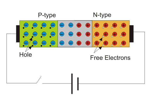
Current is carried through a semiconductor by two types of carriers: (i) free electrons which have negative charges (ii) holes that have a positive charge
In semiconductors such as silicon and germanium,there are four electrons in the outermost shell – valence electrons.
Effects of Temperature on Semiconductors
The resistance of a semiconductor will be decreasing as the temperature increases. Unlike, in the case of a pure conductor where the temperature increases with the rise in conductivity.
Types of semiconductors
- n-type semiconductor
- p-type semiconductor
n-type semiconductor: it is the addition of pentavalent element such as antimony, and germanium crystal to a semi-conductor will lead to the formation of the n-type of the semiconductor. The majority carriers are electrons and minority carriers are holes.
p-type semiconductor is produced by “doping” pure germanium or silicon crystal with an impurity or elements that have three valence electrons(trivalent),e.g., boron and indium. the majority carriers in the p-type are the positively charged holes.
The p-n junction diode
The p-n junction semiconductor is a single semiconductor made up of a p-type semiconductor and n-type semiconductors. The two types form an alloy with a fragile junction between the two semiconductor types.
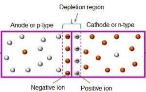
Reverse biase
In reverse biase the p-type is connected with the negative terminal while the n-type is connected to the positive terminal. This make the depletion layer to widen.
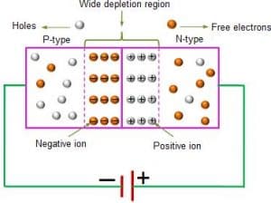
Forward biase
In forward biase the p-type is connected to the positive terminal of the battery while the n-type is connected to the negative terminal of the battery. This make the depletion layer to narrows.
Uses of p-n junction diode
- As a rectifier for alternating current and direct current voltage because its resistance can be varied from the forward biased to the reverse biased.
- The potential difference requires to operate it is small,e.g., in a radio receiver, one can use 3v of battery.
- Cheaper to manufacture
- Smaller in size
Recommended: Solutions to some UTME Physics questions